


1 rue Galilée, Espace Innova,
Parc Technologique de Soye
56270 Plœmeur, FRANCE
The electronics industry now needs precise tools to characterise circuits and to detect potential defects efficiently.
Mass production of components, as well as strict environmental and energy efficiency regulations, have led to miniaturisation and compactness of components, higher energy yields, and increased density and flexibility of component design.
Within this very broad sector, power electronics is particularly interested in our sensors.
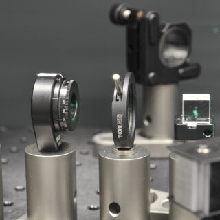
Our NV centre sensors meet these needs by providing fast measurement of electrical currents flowing in the circuit by measuring induced magnetic fields.
Coupled with CCD cameras, our sensors can image these magnetic fields, with a spatial resolution of the order of 500 nanometers, as well as currents in a wide frequency range (DC to GHz).
These essential and differentiating elements give our sensors clear competitive advantages, contributing to significant improvements in the design phase, in the efficacy of tests used in the production phase, and in energy efficacy.
Characterisation of microcircuits for quantum technologies (atom chips, quantum electrodynamics)